NEC’s contributions to the CPU market, particularly their x86 compatible V-series and later unique processors, often go unnoticed. This article delves into the history of the Nec Cpu, highlighting their innovative designs, the often forgotten FPU developments, and a mysterious discovery that sheds light on a previously unknown chapter in NEC’s CPU history.
NEC’s journey in the CPU realm began with a crucial cross-licensing agreement with Intel in 1976. This agreement allowed both companies to leverage each other’s patents, fostering a competitive landscape and enabling NEC to penetrate the Japanese market with Intel’s 8086/8088 processors. However, NEC’s ambitions extended beyond second-sourcing. They embarked on designing their own enhanced processors, leading to the creation of the V20 and V30 in 1984.
The V30, a significant advancement over the Intel 8086, featured dual 16-bit internal busses, enabling efficient data movement. This architecture, along with an expanded microinstruction word, a hardware effective address generator, and other enhancements, resulted in a more powerful and versatile NEC CPU. The V-series expanded further with the V40/V50, mimicking the Intel 80186/80188, and various microcontrollers.
Initially, the V20/V30 was intended to be paired with the upd72091 math coprocessor. However, this coprocessor was quickly deemed obsolete and canceled. Its replacement, the upd72191, was planned but never released, despite detailed specifications and motherboard designs incorporating sockets for it. The upd72191 promised significant improvements, including full IEEE-754 compatibility, an expanded instruction set, and compatibility with both the V20/V30 and V40/V50 processors.
A key feature of the upd72191 was its dual bus design, mirroring the V30 architecture, with a 74-bit mantissa bus. This wider bus, later utilized in the upd72291/72691, enabled hardware implementation of the power function (xy), a complex calculation requiring high accuracy. While the upd72191 never saw the light of day, NEC offered the upd9335C chip to facilitate interfacing the 8087 with the V40/V50 processors.
NEC’s CPU evolution continued with the V60/V70/V80 series in 1989. These processors marked a departure from the x86 architecture, featuring a completely new 32-bit ISA. The accompanying FPUs, the upd72291 and upd72691, offered impressive performance, with the latter boasting 32 floating-point registers and comprehensive matrix math capabilities.
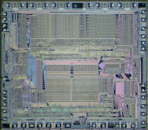
A recent discovery has added a new layer of intrigue to the history of the NEC CPU. A mysterious chip, the D9008D, was found on a board alongside a V30 processor. Analysis revealed a large die with a 74-bit mantissa processing section, indicating an FPU design. The chip’s connections and timing suggest compatibility with the V30, much like the intended functionality of the canceled upd72191. Further investigation suggests the D9008D might be a customized version of the upd72191, potentially resurrected for a specific customer application. Testing confirms that the D9008D functions as an 8087 coprocessor, at least at a basic level.
The D9008D discovery underscores the hidden depths of NEC CPU history. While many of NEC’s innovative designs were ultimately canceled, their contributions to CPU and FPU architecture remain significant. This unearthed chip serves as a reminder that even decades later, there are still technological secrets waiting to be uncovered. The story of the NEC CPU is a testament to their engineering prowess and a fascinating exploration of a lesser-known corner of computing history.